Power
A supply rail’s impedance from the regulator to the die against its target, the capacitors that bring it down, the planes’ resonances, and the droop when the load steps.
The supply’s impedance
The Power tab looks at one supply rail as the chips on it see it: an impedance between the rail and ground that must stay low enough, at every frequency the chips' current changes at, for the rail's voltage to stay within its ripple.
- Target: the rail's voltage × its allowed ripple ÷ the current step, held up to the step's knee (0.35 divided by its rise time).
- Board: a plane pair from a starter stackup (its capacitance, and the dielectric's loss), the board's size (its first cavity resonances are marked), and the spreading inductance from the capacitors to the load: the load's via pairs on a 1 mm pitch spread the current as one port of their square, plus each via's own share.
- Regulator: its output resistance and inductance. Package and die: the path from the board to the die, and the capacitance on the die.
- Capacitors: groups of capacitors with their ESR, ESL and the inductance of their pads and vias; each group's parts are in parallel. The types are typical values by size, not any maker's part: bulk (polymer), ceramic from 0201 to 1210, and low-inductance kinds (reverse geometry 0204, 0306 and 0508, interdigitated and three-terminal). ✎ on a row shows its values to change (it is then marked edited); Custom capacitor starts from your own values, and Save as my type keeps a capacitor in your library. Suggestions use the standard types and your own; tick Suggestions may use low-inductance types to let them use those too.
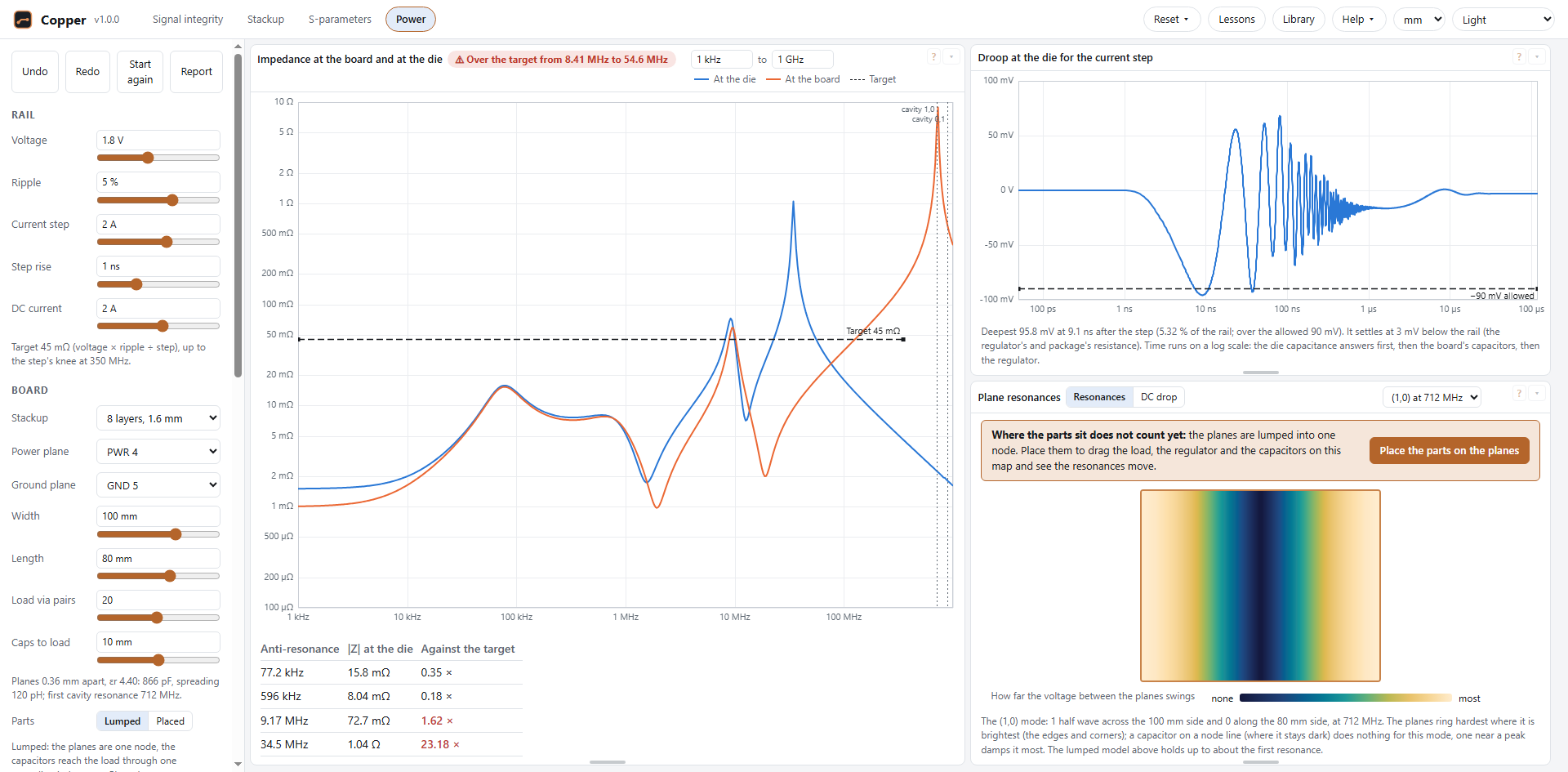
The plot gives the impedance at the board and at the die against the target; the table lists its anti-resonances (peaks between one kind of capacitor and the next). Its frequencies (1 kHz to 1 GHz at first, anything from 1 Hz to 20 GHz) are typed in its header. Suggest capacitors adds parts one at a time, each time the kind that lowers the excess over the target most, and says up to which frequency the rail then meets it: above where the package and planes alone are over the target, only capacitance on the die helps. The droop is the die's voltage after the current step, from a transient run of the same network, on a logarithmic time scale: the die capacitance answers first, then the board's capacitors, then the regulator. The run takes twenty steps to the step's rise through the fast part, then longer steps on from the same state.
The board's stackup can be a starter or one from your library. In the lumped model the plane cavity's resonances are marked, not modelled: it holds up to about the first of them.
Plane resonances shows how far the voltage between the planes swings for each of the first cavity modes, across the board's own shape: brightest at the edges and corners, dark on the node lines. A capacitor on a node line does nothing for that mode; one near a peak damps it most.
Placing the parts on the planes
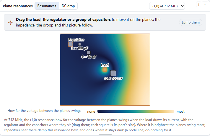
Set Parts to Placed in the sidebar, or press Place the parts on the planes above the map, and the planes become a cavity: the load, the regulator and each group of capacitors sit at a place on the board (drag them on the map under Plane resonances, use the arrow keys on one, or type where the load and the regulator are). The impedance at the board is then the planes' own at the load, with everything else where it is: the spreading inductance between each capacitor and the load, the planes' resistance, and the cavity's resonances all follow from where things are.
- The planes are worked out by the textbook mode sum for a rectangular cavity with open edges, with the copper's skin effect and resistance and the dielectric's loss. Each port is a square: the load's via pairs on a 1 mm pitch, each group's capacitors on 2 mm, the regulator 5 mm; a square port of side w acts like a via of 0.447 w across, and each via's own spreading inside its share of the square is added to its branch.
- Capacitors you have not moved sit round the load at the caps-to-load distance; bulk capacitors (10 µF and up) start by the regulator. Suggestions still come from the lumped model: place them, then look.
- The droop is then worked out from the impedance at the die itself: the step response of that impedance to the rail's current ramp.
- Plane resonances then shows how far the voltage that the load's current drives between the planes swings at each resonance, with the regulator and capacitors where they are.
Ceramics under DC bias
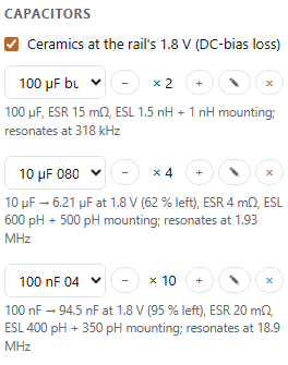
A ceramic capacitor (X5R, X7R) loses capacitance under DC voltage: a small part at its rated voltage may keep a fifth of what its label says. With Ceramics at the rail's voltage (DC-bias loss) ticked (on to start), each ceramic group works at the rail's voltage. Each type has a typical Half C at: the DC voltage at which it keeps half its capacitance (about 2.5 V for 10 µF 0805, 6 V for 1 µF 0603, 12 V for 100 nF 0402: larger values in smaller cases lose more). The capacitance kept at a voltage V is 1 / (1 + (V / Half C at)^1.5) of the label's: all of it at 0 V, half at Half C at, a quarter at about twice it.
- Each row shows its label value and what it keeps at the rail (a 10 µF 0805 on a 1.8 V rail: 6.2 µF, 62 %). Its resonance moves up as the square root of the loss, so a rail that met its target nominally can miss it.
- Set a row's Half C at from its data sheet's bias curve (✎ on the row). Empty: that part loses nothing.
- Bulk (polymer) capacitors and the die's capacitance lose nothing. Untick the box to see the label values.
The DC drop
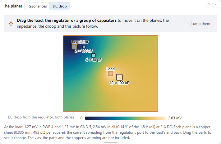
The planes are copper of finite thickness, so the load's DC current loses some voltage in them: from the regulator to the load in the power plane and back in the ground plane. Give the load's DC current (2 A to start) and set the map above the plots to DC drop (instead of Resonances).
- The map shows the drop across the board, both planes together, from 0 at the regulator to the most at the load; under it, the drop at the load in each plane and in all, and as a share of the rail's voltage.
- Each plane is a sheet of its copper's resistance per square (the copper's resistivity over its thickness: about 0.5 mΩ for 35 µm), with the current spread over the regulator's and the load's ports and insulated edges.
- The resistance between the ports is worked out exactly (a sum of the plate's modes); the map is a grid scaled to it. Both are checked against an independent solution, within 0.01 %.
- With the parts placed, drag the regulator or the load and watch the drop follow; lumped, they sit at their usual places. The vias, the parts and the copper's warming are not included.
The report
Report (above the rail) saves the rail as one page to keep, send or print: the rail and its target, the board, the regulator, package and die, every capacitor group (with its value at the rail's voltage), the anti-resonances, the DC drop, and the impedance, droop and plane pictures.